Abstract
Infrared photovoltaic cells (IRPCs) have attracted considerable attention for potential applications in wireless optical power transfer (WOPT) systems. As an efficient fiber-integrated WOPT system typically uses a 1550 nm laser beam, it is essential to tune the peak conversion efficiency of IRPCs to this wavelength. However, IRPCs based on lead sulfide (PbS) colloidal quantum dots (CQDs) with an excitonic peak of 1550 nm exhibit low short circuit current (Jsc) due to insufficient absorption under monochromatic light illumination. Here, we propose comprehensive optical engineering to optimize the device structure of IRPCs based on PbS CQDs, for 1550 nm WOPT systems. The absorption by the device is enhanced by improving the transmittance of tin-doped indium oxide (ITO) in the infrared region and by utilizing the optical resonance effect in the device. Therefore, the optimized device exhibited a high short circuit current density of 37.65 mA/cm2 under 1 sun (AM 1.5G) solar illumination and 11.91 mA/cm2 under 1550 nm illumination 17.3 mW/cm2. Furthermore, the champion device achieved a record high power conversion efficiency (PCE) of 7.17% under 1 sun illumination and 10.29% under 1550 nm illumination. The PbS CQDs IRPCs under 1550 nm illumination can even light up a liquid crystal display (LCD), demonstrating application prospects in the future.
Graphical Abstract
1 Introduction
Infrared photovoltaic cells (IRPCs) are attracting interests due to their potential applications in wireless optical power transfer (WOPT) systems, which converts the infrared laser light into electric energy (Fig. 1a and b) [1, 2]. With the increasing potential to realize long-range wireless power transfer [2,3,4,5], WOPT technology has shown great application prospects in chargers of portable electronic devices [6], sensors in the Internet of Things [7], as well as devices in industrial environments in which assembling or replacing cables is difficult [8,9,10,11]. Laser beams utilized in the WOPT system tend to have an optical fiber communication wavelength of 1550 nm [1, 11], which is safer for human eyes and is able to integrate with optical fibers. The laser beam wavelength of 1550 nm determines that the optimal bandgap of photovoltaic materials for the WOPT system is about 0.8 eV. Yet the growth of prospective materials like GaSb [12, 13] (0.73 eV) and InGaAs [14] (0.36–0.75 eV) requires ultra-high vacuum equipment and lattice-matched substrates which leads to complexity in process and high production costs. In contrast, lead sulfide colloidal quantum dots are promising materials for 1550 nm IRPCs with the advantages of bandgap tuning, high absorption coefficient, and solution processing [15].
Fig. 1
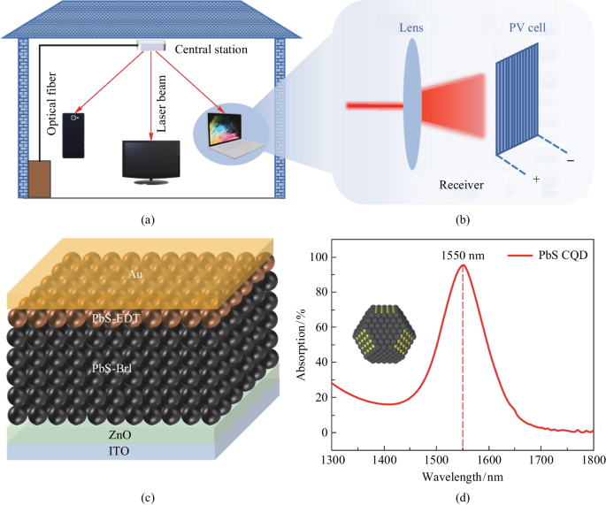
a Illustration of the WOPT technique, which is equipped with b IRPCs. c Device architecture of the PbS CQD IRPCs, and d the absorption spectrum of PbS CQD solution (2 mg/mL)
Current research on PbS CQD photovoltaic cells primarily focuses on full-spectrum solar cells and infrared solar cells pairing with silicon or perovskite cells [16,17,18,19,20,21]. Recent advances in surface passivation, device structure, and interface engineering have pushed the PCE of PbS CQD solar cells to reach 15.45% [22] and that of PbS CQD infrared solar cells to reach 11.98% [20]. Yet IRPCs required for fiber-based WOPT systems need utilize larger PbS QDs with a bandgap of ≈ 0.8 eV and a size of ≈ 5.9 nm. In the past few years, PbS CQD IRPCs with exciton absorption peaks at ~ 1550 nm, or longer wavelengths, have been developed as bottom subcells of thin-film III–V semiconductor tandem solar cells [23,24,25,26]. In 2018, the Sargent group built PbS QD solar cells using CQDs with a 0.8 eV bandgap and achieved a high external quantum efficiency (EQE) of 50% at 1550 nm [23]. In 2019, Konstantatos et al. reported photovoltaic cells using CQDs with exciton absorption peaks at 1620 nm that exhibit a high PCE of 6.4% under the full solar spectrum [26]. These devices are usually n-i-p structures with zinc oxide (ZnO) as the electron transport layer (ETL) and 1,2-ethanedithiol (EDT)-treated CQD as the hole transport layer (HTL). However, all of the reported PbS CQD IRPCs are designed to operate under the solar spectrum [17, 24, 26,27,28] whereas the absorption of IRPCs driven by monochromatic light is more sensitive to their structures. Thus, optical engineering is a vital strategy to enhance the performance of PbS-CQD-based IRPCs for fiber-based WOPT systems.
Here we developed high-performance IRPCs utilizing PbS CQDs with a peak absorption wavelength of 1550 nm. The device structure was optimized by improving ITO transmittance combined with the optical resonance effect. The champion IRPCs exhibit a high PCE of 10.29% under 1550 nm illumination (17.3 mW/cm2) and a high EQE of 51% at 1550 nm. Remarkably, this device achieved a record high PCE of 7.17% under 1 sun illumination, which is significantly higher than those reported devices that use PbS CQDs with an exciton absorption peak at 1550 nm. We further demonstrated the powering capacity of the PbS CQDs IRPCs by lighting an LCD under 1550 nm illumination.
2 Results and discussion
PbS CQDs are synthesized by a colloidal method that allows for precise band-gap engineering by size manipulation through adjusting growth kinetics and thermodynamics [15, 18, 29, 30]. The peak absorption of PbS CQDs that were utilized as the active material in this work was tuned to 1550 nm by controlling the growth time (Fig. 1d and Fig. S1b). Moreover, we adopted a cation exchange method [18] to get monodispersed PbS CQDs with fewer exposed (100) facets; this is beneficial for charge transport in the CQD film [31,32,33]. In this method, the sulfur source was ZnS CQDs synthesized by a hot injection method (Fig. S1a) and PbS CQDs were formed by the exchange of zinc cations with Pb cations in the PbCl2 solution.
We fabricated photovoltaic devices with an architecture of Glass/ITO/ZnO/PbS-1550/PbS-EDT/Au (Fig. 1c), and the device fabrication process is illustrated in Fig. 2a. We used commercial ITO as the transparent electrode and the ZnO layer deposited by magnetron sputtering as ETL for the reference devices. Then PbS CQD ink was prepared by the hybrid halide ligand strategy [19], where the native organic surface ligands were exchanged with halide anions of lead halides (PbI2:PbBr2 = 2.3:1). The QD ink was spin-coated onto the ZnO working as the photoactive layer. After that, a thin layer of EDT-treated PbS QDs with a bandgap of 1.4 eV acted as HTL. Finally, Au was deposited and worked as the top electrode.
Fig. 2
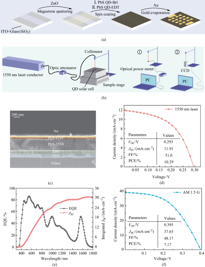
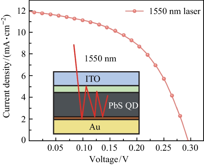
Fabrication and characterization of the IRPCs. a Overview of the device fabrication process. b System constructed to characterize the IRPC performance under 1550 nm illumination. c Cross-sectional SEM image of Glass/ITO/ZnO/PbS-1550/PbS-EDT/Au device. d Current–voltage (J–V) curves and performance parameters of the champion IRPC under 1550 nm illumination (17.3 mW/cm2). e EQE spectrum and integrated current density of the champion IRPC (no bias). f J–V curves and performance parameters of the champion IRPC under 1 sun illumination
To evaluate the PCE of the IRPCs under 1550 nm illumination, a system was self-constructed with a collimated 1550 nm fiber laser as the light source (Fig. 2b). Moreover, the system incorporated an optic attenuator to investigate the performance of the IRPC under different illumination power densities. Meanwhile, we designed a characterization scheme to determine both the power and the incident area of the laser light illuminated on the IRPC, which is essential for the accurate calculation of PCE and short circuit current (Jsc). To accurately determine the effective area of laser beam incident on the cell, we used a laser beam with a spot size that was smaller than the size of the cell. A collimating lens was employed to adjust the spot size of the laser to an area of 0.0176 cm2, as determined by a CCD camera. The cell size of the fabricated IRPCs was 0.0414 cm2.
The SEM image of the cross-section of the cell was shown in Fig. 2c, which indicated the smoothness of each functional layer. The J–V curve (under 1 sun illumination) and EQE spectrum of the reference devices are illustrated in Fig. S3. By improving ITO transmittance and utilizing the optical resonance effect, we were able to create an infrared photovoltaic cell with a high PCE of 10.29% under 1550 nm illumination (17.3 mW/cm2) and high EQE of 51.04% at 1550 nm as shown in Fig. 2d and e. Remarkably, the champion device achieved a record high PCE of 7.11% under 1 sun illumination (Fig. 2f), and performance parameters of the counterparts reported in recent years was given in Table S1. Compared with the work by the Sargent group in 2018 [23], the Jsc of our device was 50% higher; this can be attributed to the higher ITO transmittance and optical resonance effect. This high Jsc is comparable with that achieved in the work by Wang et al. in 2022 [24], but our device exhibited a higher fill factor (FF) and open circuit voltage (Voc), resulting in higher PCE. Moreover, better passivation of the QD surface and more matching ETL are expected to further improve Voc and FF.
Commercial ITO is suitable for full solar spectrum cells with high transmittance in the visible region while exhibiting low transmittance in the infrared region—specifically, lower than 30% at 1550 nm (Fig. 3a) [34,35,36]. The high concentration of free carriers in commercial ITO results in significant absorption of infrared photons and low infrared transmittance [37]. The infrared transmittance of ITO can be improved by reducing the carrier concentration. We, therefore, improved the ITO transmittance in the infrared region by magnetron sputtering ITO on the glass substrates. By tuning the amount of input oxygen during the sputtering process, the carrier concentration in the sputtered ITO was optimized to balance between transmittance and conductivity. Finally, ITO with transmittance around 81% at 1550 nm (Fig. 3a) was achieved while sacrificing the conductivity to some extent. Figure 3b shows the J–V curves of commercial ITO based and sputtered ITO-based devices under 1550 nm illumination (17.3 mW/cm2). The Jsc is significantly improved from 8.90 mA/cm2 of the commercial-ITO-based devices to 12.14 mA/cm2 of the sputtered-ITO-based ones (Table 1). Though sputtered-ITO-based devices exhibited a lower FF value due to lower conductivity, the device PCE increased from 7.89% to 8.77%, with a net increase of 0.88%. These results indicate that the transmittance of ITO is a more crucial factor than its conductivity for the efficiency of IRPCs when operating under 1550 nm laser illumination.
Fig. 3
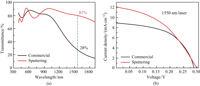
Device optimization through ITO transmittance. a Transmittance spectra of commercial ITO and sputtered ITO. b J–V curves of the devices based on commercial and sputtered ITO under 1550 nm illumination (17.3 mW/cm2)
Table 1 Performance parameters of CM/SP ITO devices under 1550 nm laser illuminationWe further enhanced absorption of the IRPC device by utilizing the optical resonance effect for the WOPT systems operating under 1550 nm illumination. The absorption can be increased when the thickness of each layer is well-matched [16, 38]. We used the finite element method (FEM) to calculate the absorption characteristics of the device for different thicknesses of the ZnO layer. The simulation model is illustrated in Fig. 4a, which has 6 layers: Glass (1.1 mm), ITO (280 nm), ZnO (0–500 nm), PbS (450 nm), EDT-PbS (46 nm), and Au (60 nm). Figure 4b shows the calculated absorption of the device as a function of ZnO thickness under 1550 nm illumination. Within the ZnO layer thickness range of 0–500 nm, the device shows a calculated peak absorption of 65% when the ZnO thickness is around 170 nm.
Fig. 4
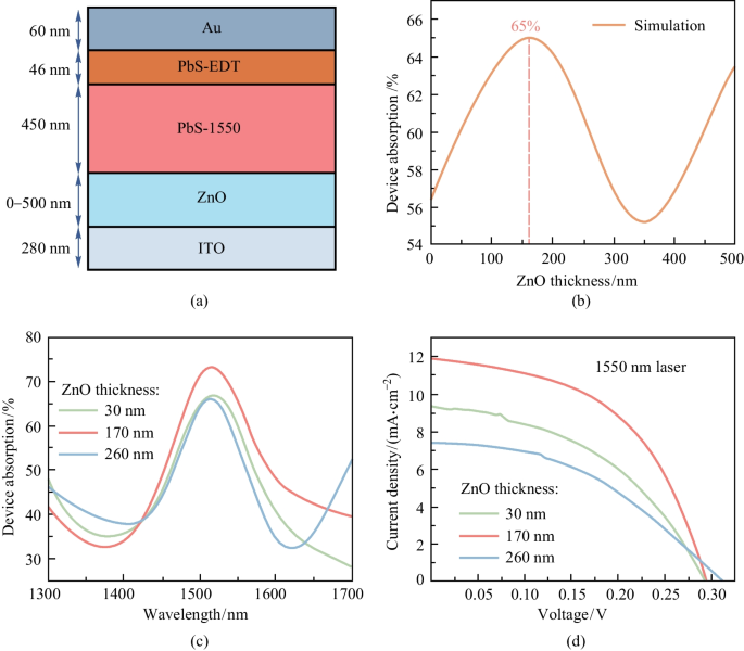
Device optimization through the optical resonance effect. a Illustration of the device cross-section with different ZnO thicknesses in the range of 0–500 nm. b Calculated absorption at 1550 nm as a function of ZnO layer thickness. c Absorption spectra of devices with various thicknesses of the ZnO layer. d J–V curves of devices with various thicknesses of ZnO layer under 1550 nm laser illumination (17.3 mW/cm2)
To further verify the simulation results, the ZnO layers with various thicknesses were prepared on ITO substrates by controlling the sputtering time. When the thickness of the ZnO layer ranged from 30 to 260 nm, good agreement between experimental results and calculations was observed. Figure 4c shows that the device with a ZnO layer thickness of 170 nm exhibited more significant absorption enhancement at an incident wavelength of 1550 nm, compared with devices with ZnO layer thickness of 30 and 260 nm. These results indicated that the optical resonance effect was enhanced in devices with a suitable ZnO layer thickness. As expected, the absorption enhancement enabled the increase of current density (Fig. 4d), and devices with a ZnO layer thickness of 170 nm exhibited higher FF (Table 2). We attribute this to the enhanced carrier extraction compared with that for the devices with a 30 nm ZnO layer; as well as better carrier transport in the ETL compared with that for the devices with a 260 nm ZnO layer. The relationship between ZnO depletion region width (WZnO) and QD depletion region width (WQD) can be illustrated as [16]
�ZnO�ZnO=�QD�QD,
where NZnO is ZnO dopant concentration and NQD is QD dopant concentration. With the increase of ZnO thickness, the QD depletion region is widened and the carrier extraction ability is improved. However, too thick a ZnO layer will make it difficult for extracted carriers to cross the ETL. Due to the significantly improved Jsc and FF, the PCE of the optimized device was 10.29%, which was 3.24% and 4.63% higher than that of the devices with 30 and 260 nm ZnO layer, respectively. Thus, devices with a ZnO layer thickness of 170 nm demonstrated superior infrared light conversion capability due to the optical resonance effect.
Table 2 Performance parameters of devices with various thicknesses of ZnO layer under 1550 nm laser illumination
We further investigated the performances of the optimized devices under various power intensities of the incident laser light. With the light power intensity changing from 10 to 300 mW/cm2 (Fig. S6), we observed that the Jsc and maximum power output increased along with increasing laser intensity; the rate of increase became lower at high light intensities. Figure <a href="https://link.springer.com/article/10.
